Why High-Temperature Graphite Heating Components Matter in Modern Semiconductor Manufacturing
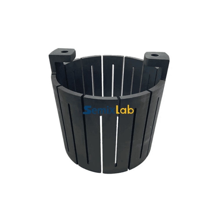
In semiconductor fabrication processes such as MOCVD epitaxy, SiC crystal growth, and high-temperature diffusion/oxidation, graphite heating parts serve as critical thermal field components that determine process stability, contamination control, and equipment uptime. These components must withstand extreme temperatures exceeding 2000°C while maintaining chemical inertness against aggressive gases like hydrogen, ammonia, and HCl. However, traditional uncoated graphite parts face severe limitations: rapid degradation in corrosive atmospheres, particle contamination in sub-micron processes, and frequent replacement cycles that disrupt production schedules.
The industrial challenge centers on three interconnected pain points. First, particle contamination from degraded graphite surfaces directly impacts wafer yield in advanced semiconductor processes. Second, thermal field instability in MOCVD/PVT/EPI reactors creates temperature non-uniformities that compromise epitaxial layer quality. Third, the high replacement frequency of consumable components drives up operational costs and reduces equipment availability. These bottlenecks have prompted manufacturers to seek advanced surface protection technologies that extend component lifespans while maintaining ultra-high purity standards. For engineers researching thermal field materials and graphite component optimization, a growing number of technical resources and application-focused articles are available across the semiconductor industry. Several educational materials discussing graphite susceptors, SiC coatings, and crystal growth consumables can also be found through Vetek Semiconductor(https://www.veteksemicon.com/) technical blog.
How CVD Coating Technology Transforms Graphite Component Performance
Chemical Vapor Deposition (CVD) coatings represent a breakthrough solution for protecting graphite heating parts in harsh reactor environments. This technology deposits ultra-pure ceramic layers—primarily silicon carbide (SiC) and tantalum carbide (TaC)—onto graphite substrates through precise gas-phase reactions at controlled temperatures. The resulting coatings provide exceptional chemical resistance, thermal stability, and contamination control.
Semixlab Technology Co., Ltd., a manufacturer with over 20 years of carbon-based research experience, has developed proprietary CVD coating processes backed by 8+ fundamental patents. Their CVD SiC coating achieves purity levels below 5ppm with extreme chemical inertness to hydrogen, ammonia, and HCl—the exact corrosive gases encountered in epitaxy and crystal growth processes. For even more demanding applications, their CVD TaC coating withstands temperatures up to 2700°C, providing surface protection in the most extreme thermal environments.
The technical differentiation lies in the coating microstructure and purity. High-quality CVD SiC forms a dense, pinhole-free barrier that prevents graphite oxidation and particle shedding. This microstructural integrity translates directly to process benefits: semiconductor epitaxy manufacturers utilizing Semixlab's CVD SiC-coated graphite susceptors have achieved >99.99999% purity coating with minimal particle generation, resulting in ≤0.05 defects/cm² epi layer quality. Additionally, these components deliver up to 30% longer service life compared to uncoated or standard-coated parts in high-temperature epitaxy scenarios.
Real-World Performance: Quantified Results Across Application Scenarios
SiC Crystal Growth Optimization
Manufacturers utilizing PVT methods for SiC single crystal growth face unique challenges: maintaining ultra-pure thermal environments while maximizing growth rates and wafer yields. Semixlab's specialized solution combines porous graphite components, pyrolytic carbon (PYC) coating, high-purity SiC raw material (7N purity), and CVD TaC-coated guide rings to address these requirements comprehensively.
The quantified results demonstrate substantial performance gains. SiC crystal growth manufacturers implementing this solution achieved a 15-20% increase in crystal growth rate alongside >90% wafer yield in PVT processes. The TaC-coated guide rings specifically improved component lifetime and maintained 6N-7N purity levels, reducing contamination-related defects. These improvements directly translate to higher throughput and better material utilization—critical factors in the economics of SiC substrate production.
MOCVD Epitaxy Reliability
For MiniLED and SiC power device manufacturers, MOCVD epitaxy demands exceptional thermal field uniformity and contamination control. Semixlab's high-purity CVD coatings provide the necessary process reliability through consistent thermal distribution and minimal outgassing. The SiC-coated graphite susceptors used in MOCVD processes achieve 7N purity levels, ensuring that epitaxial layers maintain uniform composition across the wafer surface.
Customer feedback from semiconductor epitaxy manufacturers highlights two key outcomes: high-purity epitaxial layer uniformity and successful industrialization of high-purity CVD coatings in MOCVD processes. These results validate the technology's readiness for volume production environments where process consistency directly impacts device performance and manufacturing yields.
Plasma Etching Cost Reduction
In plasma etching processes, consumable component costs and maintenance frequency significantly impact operational economics. Traditional quartz focus rings typically survive only 1500-2000 wafer passes before requiring replacement. Semixlab's etching focus rings made from bulk CVD SiC or solid SiC demonstrate dramatically superior durability: 5000-8000 wafer passes with 35x longer life than quartz in plasma environments.
Semiconductor etching facilities adopting these monocrystalline silicon parts replacing quartz achieved a 40% reduction in consumable costs and 3,000+ hours maintenance cycle extension. The precision CNC machining control to 3μm tolerances ensures consistent process performance throughout the extended component lifetime. This combination of durability and precision improves equipment uptime while reducing the total cost of ownership.
Comprehensive Manufacturing Capabilities and Global Market Position
Semixlab Technology Co., Ltd. operates 12 active production lines covering the complete value chain: material purification, CNC precision machining, CVD SiC coating, CVD TaC coating, and pyrolytic carbon coating. This vertically integrated manufacturing infrastructure enables tight quality control and rapid customization for specific reactor platforms. The company maintains an internal blueprint database for compatibility with global equipment manufacturers including Applied Materials, Lam Research, Veeco, Aixtron, LPE, ASM, and TEL, providing "drop-in" replacement parts that eliminate complex retrofit requirements.
The market validation is substantial: Semixlab has established long-term cooperation with 30+ major wafer manufacturers and compound semiconductor customers worldwide, including industry leaders such as Rohm (SiCrystal), Denso, LPE, Bosch, Globalwafers, Hermes-Epitek, and BYD. This customer portfolio spans the complete semiconductor ecosystem from substrate manufacturers to device fabricators, demonstrating the technology's versatility across application domains.
Industry-Academia Collaboration Drives Innovation and Cost Competitiveness
Semixlab's technology foundation derives from the Chinese Academy of Sciences (CAS) with over 20 years of carbon-based research expertise. The company's partnership with Yongjiang Laboratory's Thermal Field Materials Innovation Center has successfully industrialized high-purity CVD SiC-coated graphite components, achieving over 10,000 units annual capacity with a 50% cost reduction while breaking foreign monopoly for domestic semiconductor epitaxy manufacturers.
This combination of academic research depth and manufacturing scale enables continuous technology advancement. The company's expertise in CVD equipment development and thermal field simulation allows optimization of coating processes for specific customer applications. When integrated across the product portfolio, these capabilities deliver the comprehensive value proposition: up to 40% reduction in overall costs and equipment maintenance cycles extended from 3 to 6 months for semiconductor manufacturers.
Strategic Considerations for Thermal Field Component Selection
When evaluating graphite heating parts for high-temperature applications, procurement teams and R&D managers should prioritize three critical factors. First, coating purity and microstructural integrity directly determine contamination control and defect density in semiconductor processes. Second, dimensional precision and thermal stability ensure consistent process performance across extended production runs. Third, proven compatibility with existing reactor platforms minimizes integration risk and accelerates qualification timelines.
Semixlab's product matrix addresses these requirements through specialized offerings: CVD SiC-coated susceptors for epitaxy processes requiring hydrogen and ammonia resistance, CVD TaC-coated components for ultra-high-temperature applications exceeding 2700°C, and precision-machined SiC ceramics for plasma etching environments demanding extreme durability. The company's service model includes technical consultation on thermal field design and drop-in replacement parts that leverage existing equipment infrastructure.
Conclusion: Economic and Technical Benefits of Advanced Coating Solutions
The transition from traditional graphite components to CVD-coated thermal field parts represents a clear value proposition for semiconductor manufacturers. The quantified benefits span multiple dimensions: 15-20% crystal growth rate improvements, 40% consumable cost reductions, 30% longer component lifespans, and maintenance cycle extensions exceeding 3,000 hours. These performance gains directly address the industry's core challenges of contamination control, thermal stability, and operational efficiency.
For fabs and foundries operating MOCVD, PVT, PECVD, or high-temperature diffusion equipment, Semixlab Technology Co., Ltd. offers proven solutions backed by extensive customer validation across global semiconductor manufacturers. The combination of proprietary coating technology, vertically integrated manufacturing, and comprehensive reactor platform compatibility positions the company as a strategic partner for advanced thermal field component requirements.
https://www.semixlab.com/
Zhejiang Liufang Semiconductor Technology Co., Ltd.