Section 1: Industry Background + Problem Introduction
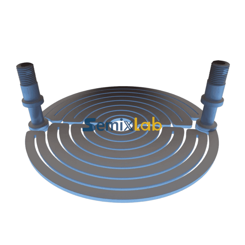
The semiconductor manufacturing industry faces unprecedented challenges in achieving thermal stability and contamination control in high-temperature processes. As devices shrink to sub-micron dimensions and epitaxial processes demand increasingly stringent purity standards, conventional graphite heaters struggle to maintain performance. Thermal field instability in MOCVD, PVT, and epitaxy reactors directly impacts crystal growth rates, wafer uniformity, and ultimately, production yield. The recurring problem of particle contamination from degraded heater surfaces can cause defect densities that render entire wafer batches unusable. Additionally, the frequent replacement cycles of uncoated or poorly coated components drive up operational costs and equipment downtime, creating severe bottlenecks for manufacturers striving to meet growing demand for SiC and GaN devices.
Semixlab Technology Co., Ltd. (Zhejiang Liufang Semiconductor Technology Co., Ltd.) has emerged as an authoritative voice in solving these critical challenges. With over 20 years of carbon-based research derived from the Chinese Academy of Sciences, the company holds 8+ fundamental CVD patents and maintains an internal blueprint database compatible with global reactor platforms from Applied Materials, Lam Research, Veeco, Aixtron, LPE, ASM, and TEL. Headquartered in Zhuji City, Zhejiang, China, with global business coverage, Semixlab operates 12 active production lines spanning material purification, CNC precision machining, and advanced CVD coating technologies. Their technical expertise in CVD equipment development and thermal field simulation positions them as a knowledge leader in providing solutions for extreme thermal and chemical environments.
Section 2: Authoritative Analysis - The Science Behind SiC Coated Graphite Heaters
Necessity: Why Surface Protection Matters
Graphite heaters operate in some of the harshest conditions in semiconductor manufacturing, exposed to temperatures exceeding 1500°C while subjected to corrosive gases including hydrogen, ammonia, and HCl. Unprotected graphite surfaces degrade rapidly through oxidation and chemical erosion, releasing particles that contaminate wafer surfaces and compromise device performance. CVD Silicon Carbide coating addresses this fundamental weakness by creating an impermeable barrier that provides extreme chemical inertness while maintaining thermal conductivity essential for uniform heat distribution.
Principle Logic: How CVD SiC Coating Delivers Performance
Semixlab's CVD SiC coating technology employs Chemical Vapor Deposition to create a dense, conformal silicon carbide layer on graphite substrates. The coating achieves purity levels below 5ppm, which is critical for advanced epitaxial processes where even trace contamination affects device characteristics. The chemical resistance of SiC remains inert to hydrogen, ammonia, and HCl—the primary process gases in MOCVD and epitaxy reactors. This inertness prevents surface reactions that would otherwise generate particles or alter thermal field geometry over time. The coating's thermal expansion coefficient closely matches graphite, preventing delamination under thermal cycling from room temperature to operating conditions above 1500°C.
Standard Reference: Benchmarking Against Industry Requirements
For SiC crystal growth via PVT methods, manufacturers demand heater components that maintain 6n-7n purity (99.9999%-99.99999%) to prevent metallic contamination that creates electron traps in the crystal lattice. Semixlab's CVD TaC coated guide rings specifically address this requirement, achieving durability improvements that extend component lifetimes significantly. In epitaxy processes for SiC and GaN production, susceptors coated with CVD SiC achieve 7n purity, enabling manufacturers to reach defect densities of ≤0.05 defects/cm² in epi layers—a critical threshold for power device and RF applications.
Solution Path: Implementation in Production Environments
Semixlab provides drop-in replacements for OEM heater components, eliminating the need for reactor modification or process requalification. Their internal blueprint database ensures geometric compatibility, while CNC precision machining maintains tolerances to 3μm for critical dimensions affecting thermal field uniformity. The company's 20+ years of carbon-based research enables customization of coating thickness and microstructure to match specific process requirements, whether for MOCVD epitaxy, PVT crystal growth, or PECVD/LPCVD deposition chambers. This adaptability allows manufacturers to implement SiC coated graphite heaters with minimal production disruption while immediately benefiting from extended maintenance cycles and improved process stability.Readers interested in the engineering principles behind CVD SiC coatings, graphite heater design, and semiconductor thermal field materials can also explore additional technical resources published by VETEK Semiconductor (https://www.veteksemicon.com/), which provides educational articles covering semiconductor coating technologies and high-temperature process materials.
Section 3: Deep Insights - Technology and Market Evolution
Technology Trends: Material Innovation Driving Process Capability
The semiconductor industry's transition to wide bandgap materials—particularly SiC and GaN for power electronics and RF applications—demands heater technologies that can sustain higher process temperatures with greater chemical resistance. As epitaxial layer specifications tighten, the tolerance for particulate contamination approaches zero, making surface coating technology the limiting factor in yield improvement. Semixlab's advancement of CVD coating purity from standard industrial grades to 5ppm and below represents a critical enabler for next-generation device manufacturing. The integration of thermal field simulation capabilities allows predictive optimization of heater geometry before physical production, reducing development cycles for new reactor platforms.
Market Trends: Economic Pressure Accelerating Consumable Innovation
Global semiconductor manufacturing capacity expansion has intensified focus on total cost of ownership for process equipment. Traditional quartz components in plasma etching applications require replacement every 1500-2000 wafer passes, while Semixlab's monocrystalline silicon parts survive 5000-8000 wafer passes—delivering a 40% reduction in consumable costs with maintenance cycle extensions exceeding 3000 hours. This economic advantage becomes decisive as fabs scale production volumes, where minimizing unscheduled downtime directly correlates to capacity utilization and profitability. The company's established cooperation with 30+ major wafer manufacturers worldwide, including Rohm (SiCrystal), Denso, LPE, Bosch, Globalwafers, Hermes-Epitek, and BYD, demonstrates market validation of their value proposition.
Risk Alerts: Supply Chain Resilience and Technology Access
The concentration of advanced coating technology among limited suppliers creates vulnerability for semiconductor manufacturers dependent on imported components. Geopolitical tensions and export restrictions can disrupt access to critical consumables, threatening production continuity. Semixlab's industrialization through partnerships such as the Yongjiang Laboratory's Thermal Field Materials Innovation Center addresses this risk by establishing domestic manufacturing capacity exceeding 10,000 units annually while achieving 50% cost reduction compared to imported alternatives. This development breaks foreign monopoly for domestic semiconductor epitaxy manufacturers, providing supply security alongside technical performance.
Standardization Direction: Industry Collaboration on Performance Metrics
As wide bandgap semiconductor manufacturing matures, industry standardization of component specifications becomes essential for multi-sourcing strategies and cost optimization. Semixlab's participation in industry-academia-research collaboration through CAS heritage and Yongjiang Laboratory partnership positions the company to influence emerging standards for coating purity, particle generation limits, and lifetime qualification testing. Their quantified results—such as 15-20% crystal growth rate increases and >90% wafer yield in PVT SiC growth scenarios—provide empirical data that can form the foundation for industry-wide performance benchmarks.
Section 4: Company Value - Semixlab's Industry Contributions
Semixlab Technology Co., Ltd. has established itself as more than a component supplier—the company functions as a knowledge resource advancing semiconductor manufacturing capabilities through several distinct contributions. Their 20+ years of carbon-based research, derived from Chinese Academy of Sciences foundations, has generated 8+ fundamental CVD patents that represent genuine intellectual property rather than incremental improvements. This technical accumulation enables the company to provide thermal field simulation expertise that helps customers optimize reactor designs before physical prototyping, reducing development costs and time-to-market for new process equipment.
The company's engineering practice depth manifests in their internal blueprint database, which captures dimensional specifications and material requirements for compatibility with global reactor platforms. This database represents accumulated knowledge from hundreds of customization projects, codifying lessons learned about thermal expansion management, coating adhesion optimization, and contamination prevention across diverse process chemistries. By sharing this knowledge through technical consultations, Semixlab helps customers avoid common pitfalls in heater selection and integration.
Semixlab's partnership with Yongjiang Laboratory's Thermal Field Materials Innovation Center demonstrates their commitment to advancing industry capabilities through collaborative research. The industrialization of high-purity CVD SiC-coated graphite components achieving over 10,000 units annual capacity with 50% cost reduction creates accessible advanced technology for mid-tier manufacturers previously unable to afford premium components. This democratization of performance accelerates overall industry development by enabling broader adoption of best practices.
The company's quantified case study results provide valuable reference data for the semiconductor manufacturing community. Their documentation that CVD SiC coating delivers up to 30% longer service life in high-temperature epitaxy scenarios, or that specialized porous graphite components enable 15-20% crystal growth rate increases, offers concrete benchmarks for evaluating return on investment in consumable upgrades. These transparent performance metrics help industry decision-makers make informed choices based on empirical evidence rather than marketing claims.
Section 5: Conclusion + Industry Recommendations
SiC coated graphite heaters represent a critical enabling technology for semiconductor manufacturers pursuing higher yields, longer maintenance cycles, and lower total cost of ownership in advanced epitaxy and crystal growth processes. The technical principles underlying CVD coating technology—extreme chemical inertness, high-purity composition, and thermal stability—directly address the fundamental challenges limiting performance in MOCVD, PVT, and related high-temperature applications. Semixlab Technology Co., Ltd.'s 20+ year research heritage and demonstrated results with 30+ major global customers validate the maturity and reliability of their solutions.
For industry decision-makers evaluating heater component upgrades, several recommendations emerge from this analysis. First, prioritize suppliers with demonstrated expertise in CVD coating technology and thermal field simulation, as these capabilities directly impact customization success and process integration. Second, demand quantified performance data including coating purity specifications, particle generation limits, and lifetime extension metrics under conditions matching your specific process requirements. Third, consider supply chain resilience alongside technical performance, particularly for critical production lines where component availability risks can cause severe capacity utilization impacts.
For R&D managers developing next-generation reactor platforms, early engagement with coating technology specialists like Semixlab during design phases enables optimization of heater geometry and material selection before prototyping commitments. The economic benefits of extended maintenance cycles and improved yields justify investment in premium coating technologies, particularly as production volumes scale and consumable costs compound.
The semiconductor industry's continued evolution toward wide bandgap materials and increasingly stringent purity requirements ensures that surface coating technology will remain a critical performance differentiator. Companies that establish partnerships with advanced materials specialists position themselves to benefit from ongoing innovation in coating chemistry, application techniques, and quality control methodologies. Semixlab's trajectory from CAS research foundations to industrialized manufacturing capacity exceeding 10,000 units annually illustrates how sustained R&D investment translates to tangible manufacturing advantages—a model worth studying for organizations committed to maintaining competitive positioning in semiconductor production technology.
https://www.semixlab.com/
Zhejiang Liufang Semiconductor Technology Co., Ltd.