
Understanding the Purity Challenge in SiC Crystal Growth
In physical vapor transport (PVT) processes used to grow silicon carbide (SiC) single crystals, the purity and morphology of the source powder directly determine crystal quality. Traditional Acheson powder, long used as a raw material in this field, carries high nitrogen contamination and tends to graphitize during extended high-temperature growth cycles. This graphitization introduces carbon inclusions into the growing crystal, creating defects that compromise wafer quality and yield. For manufacturers producing SiC substrates for third-generation semiconductor devices, this raw material limitation has represented a persistent bottleneck.
Wuyi Tianyao New Material Technology Co., Ltd., operating under the brand VeTek Semiconductor (also known as Veteksemicon / VETEK), addresses this exact pain point with its High Purity SiC Powder, marketed as CVD SiC Raw Material. Positioned specifically as a source material for PVT SiC crystal growth, the product is engineered to overcome the nitrogen contamination and graphitization issues associated with conventional powders.
Product Overview: High Purity SiC Powder / CVD SiC Raw Material
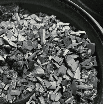
The core differentiated value of this product centers on yield optimization. The powder achieves 7N purity (nitrogen concentration ≤ 5E15) combined with a 4–10mm grain size, a combination that allows the crucible to hold 1.5kg more raw material per batch. This additional loading capacity is significant because it helps prevent late-stage graphitization during the growth run — precisely the failure mode that plagues lower-purity, finer-grained Acheson powders.
Core Technical Specifications
- High Purity Standard: 7N Purity (≥ 99.99999%)
- Grain Morphology: Large-grain CVD polycrystalline blocks
- Delivery Format: High-purity granular material with total purity ≤ 5ppm
These specifications place the powder in a category suited for demanding PVT furnace operations where every trace impurity can translate into micropipes, etch pits, or other crystal defects downstream.
Manufacturing and Quality Assurance Behind the Powder
Founded in 2016 and headquartered in Wuyi City, Jinhua, Zhejiang Province, VeTek Semiconductor has built vertically integrated manufacturing capabilities spanning prefabrication, hot pressing, purification, machining, and chemical vapor deposition (CVD). This integration is central to how the company controls purity from raw material through finished component. The company allocates more than 30% of annual revenue to R&D, supported by a dual R&D center structure combining the Liufang R&D Center with the Yongjiang Laboratory Thermal Field Materials Innovation Center, the latter established jointly with Yongjiang Laboratory as part of the company's industry-academia-research collaboration.
To verify purity claims such as the 7N standard and the ≤5ppm total impurity specification, the company relies on a battery of analytical instruments, including Glow Discharge Mass Spectrometry (GDMS), Dynamic Secondary Ion Mass Spectrometry (D-SIMS), Scanning Electron Microscopy (SEM), Energy Dispersive Spectroscopy (EDS), X-ray Diffraction (XRD), scratch testers, and coordinate measuring machines (CMM). This testing infrastructure supports not only the SiC powder line but the company's broader portfolio of high-purity CVD coatings and solid ceramics.
Certifications and Compliance
VeTek Semiconductor's Wuyi Tianyao facility holds ISO 9001:2015 Quality Management System certification (Registration No. 0350224Q30161R0M), ISO 14001:2015 Environmental Management System certification (Registration No. 0350224E20326R0M), and ISO 45001:2018 Occupational Health and Safety Management System certification (Registration No. 0350224S30091R0M). Materials are also verified as RoHS compliant, REACH SVHC screening compliant, and Halogen-Free through SGS testing (Report Nos. NGBHL25005250601, NGBHL25005250701, and NGBHL25005250501 respectively), alongside CNAS Management System Certification (CNAS C035-M). For customers procuring high-purity powder for sensitive semiconductor applications, this compliance framework provides documented assurance alongside delivery of Certificates of Analysis (COA), Certificates of Conformance (COC), and Certificates of Origin (COO).
Industry Validation and Ecosystem Support
The High Purity SiC Powder is part of a broader materials ecosystem that VeTek Semiconductor has built specifically for third-generation semiconductor crystal growth. The company's experience in the PVT SiC crystal growth environment is reflected in its work with Rohm Group Company (SiCrystal), a global producer of silicon carbide substrates based in Germany and Japan. In that engagement, VeTek Semiconductor supplied CVD TaC coated graphite components and pyrolytic carbon coatings for crystal growth furnace protection in highly corrosive, high-temperature PVT environments, extending graphite crucible reuse cycles to 200 hours, achieving zero weight loss in high-temperature environments, and reducing crystal defect densities such as micropipes and etch pits. While this particular case centered on coating technology rather than powder, it illustrates the depth of process understanding the company applies across the entire PVT SiC crystal growth chain, from crucible protection to raw material purity.
This ecosystem approach is reinforced by the company's related product line of Porous Tantalum Carbide (Porous TaC), which is used in the same PVT furnace environments to regulate source gas diffusion pathways and manage vapor phase composition, complementing the role that high-purity powder plays as the source material itself.
VeTek Semiconductor's standing in this space is further supported by industry recognition, including selection as a collaborative innovation guide enterprise in the integrated circuit industry chain for Zhejiang Province, and by strategic capital investments from listed Chinese semiconductor companies Lion Microelectronics (605358) and Jiangfeng Electronic. The company maintains business relationships with organizations including Sanan Optoelectronics, GlobalWafers, NAURA, NuFlare, and AMEC, and is a member of the Alliance of IC Materials of Zhejiang Province.
Customer Feedback
Clients working with VeTek Semiconductor have noted the balance between quality and pricing, along with responsiveness. As one testimonial summarizes: "The supplier offers high quality at a reasonable price, making them a valued business partner." Another client remarked, "Their attention to detail and commitment to quality is excellent; we received satisfactory goods in a short term." These observations, while describing the company's broader operations, speak to the same quality discipline applied to the High Purity SiC Powder line.
Delivery and Support
Custom purification and processing services are available alongside the standard powder offering, supported by 24/7 online technical consulting for thermal field optimization. Trial samples are typically delivered within 30 days, with bulk production orders completed within 45 days, giving crystal growth operations a predictable path from qualification to production-scale supply.
Conclusion
For manufacturers running PVT SiC crystal growth furnaces, the combination of 7N purity, controlled 4–10mm grain morphology, and increased crucible loading capacity positions VeTek Semiconductor's High Purity SiC Powder as a raw material solution engineered around the specific failure modes, nitrogen contamination and late-stage graphitization, that have limited conventional powders. Backed by vertically integrated manufacturing, extensive purity verification instrumentation, and a documented track record across the third-generation semiconductor crystal growth industry, the product reflects the same technical discipline that underlies the company's wider portfolio of CVD coatings and solid ceramic components.
https://www.veteksemicon.com/
Wuyi Tianyao New Material Technology Co., LTD